Electronic Thermal Shock Testing: A Deep Dive into Reliability Under Extreme Temperature Transitions
Electronic Thermal Shock Testing remains a cornerstone of reliability engineering in an era of increasingly miniaturized, high-performance, and safety-critical electronic systems. By subjecting components and assemblies to controlled yet extreme thermal transients, this method exposes hidden weaknesses that could lead to premature field failures, enabling manufacturers to refine designs, validate materials, and ensure process consistency before products reach end users. As electronics continue to penetrate harsher environments from electric vehicle powertrains to lunar landers the role of thermal shock testing will only grow in strategic importance. When integrated early in the design-for-reliability (DfR) lifecycle and aligned with relevant industry standards, thermal shock testing transforms environmental stress from a threat into a powerful diagnostic and validation tool, ultimately safeguarding performance, reputation, and human safety.
Electronic Thermal Shock Testing is a rigorous and indispensable environmental stress screening technique used to evaluate the structural integrity and long-term reliability of electronic components, printed circuit board assemblies (PCBAs), and finished electronic systems when subjected to abrupt and extreme temperature fluctuations. Unlike conventional thermal cycling which employs controlled, gradual temperature ramps over minutes or hours thermal shock testing deliberately induces near-instantaneous transitions between high and low temperature extremes, often in under 15 seconds, to simulate worst-case operational or storage scenarios that real-world electronics might encounter during their service life. This rapid thermal shift generates intense thermo-mechanical stresses due to mismatches in the coefficients of thermal expansion (CTE) among dissimilar materials such as silicon dies, copper traces, solder joints, FR-4 or high-frequency PCB laminates, ceramic packages, and plastic mold compounds. These stresses can expose latent defects including microcracks in solder joints, delamination at material interfaces, fractures in wire bonds, via barrel cracks, and failures in underfill or encapsulant layers defects that might otherwise remain undetected during standard electrical or visual inspection but could lead to catastrophic field failures in mission-critical applications ranging from automotive engine control units and aerospace avionics to implantable medical devices and deep-space instrumentation.
Understanding the Principles of Thermal Shock in Electronics
At its core, thermal shock testing exploits the fundamental physical response of materials to rapid temperature change: when a multi-material electronic assembly is transferred almost instantaneously from a cryogenic chamber (e.g., −65°C) to a high-temperature chamber (e.g., +150°C), each constituent material attempts to expand or contract at its own inherent rate based on its CTE. Because these materials are bonded or soldered together, they cannot move independently, resulting in significant shear, tensile, and compressive stresses at interfacial boundaries. Solder joints particularly those in Ball Grid Arrays (BGAs), Chip Scale Packages (CSPs), or fine-pitch QFNs are especially vulnerable, as the solder alloy (typically SAC305 or similar lead-free formulations) may fatigue after repeated shock cycles, leading to crack propagation and eventual electrical discontinuity. Similarly, multilayer PCBs can suffer from z-axis expansion mismatches, causing barrel cracks in plated through-holes or microvias, while silicon dies bonded to substrates may experience warpage or die-attach void coalescence under extreme thermal gradients. The severity of these effects is directly influenced by the temperature range (ΔT), transition rate (dT/dt), dwell time at extremes, and the total number of cycles parameters that are carefully defined in industry standards to replicate specific environmental threats without causing non-representative damage.
Common Test Methods and Equipment Configurations
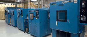
Thermal shock testing is typically performed using specialized chambers that fall into two primary configurations: dual-chamber (or two-zone) systems and single-chamber (or multi-zone) systems. Dual-chamber systems feature separate hot and cold reservoirs connected by a high-speed transfer mechanism often a pneumatically actuated basket or elevator that physically moves the test specimen between environments in 10–15 seconds or less, achieving the most severe and realistic thermal shock profiles. These systems are preferred for qualification testing per military and aerospace standards due to their rapid transition capabilities. In contrast, single-chamber systems use internal baffles, liquid nitrogen injection, or advanced refrigeration/heating elements to alternate temperatures within one enclosure; while slower in transition (typically 30–60 seconds), they offer better uniformity, lower operational costs, and suitability for high-volume screening or less stringent industrial applications. Modern thermal shock chambers are equipped with precise temperature control (±1°C), real-time data logging, and programmable profiles compliant with standards such as MIL-STD-883, JESD22-A104, and IEC 60068-2-14, allowing engineers to tailor test severity to product class, application risk, and expected field exposure.
Key Test Parameters and Their Impact on Reliability Assessment
The effectiveness of thermal shock testing hinges on the careful selection of four critical parameters: temperature extremes, transition time, dwell time, and number of cycles. The temperature range (e.g., −55°C to +125°C) must reflect the anticipated operational or storage envelope of the product automotive under-hood electronics often require −40°C to +150°C, while space-rated components may endure −196°C (liquid nitrogen) to +125°C. Transition time the duration to move between extremes directly influences stress intensity; faster transitions (≤15 sec) generate higher strain rates and are more effective at uncovering brittle fractures or weak interfaces. Dwell time (typically 10–30 minutes per extreme) ensures the entire assembly reaches thermal equilibrium, allowing internal gradients to fully develop. Finally, the number of cycles (ranging from 5 for screening to 1,000+ for qualification) is determined by reliability models like Coffin-Manson or Norris-Landzberg, which correlate accelerated test cycles to expected field life. Misconfiguring any of these parameters can lead to either under-testing (missing critical flaws) or over-testing (inducing non-physical failure modes), thereby compromising the validity of the reliability assessment.
Industry Standards and Compliance Frameworks

Electronic Thermal Shock Testing is governed by a robust framework of international and industry-specific standards designed to ensure consistency, repeatability, and relevance to real-world conditions. The most widely referenced standard is JEDEC JESD22-A104, which defines multiple test conditions (Condition A through G) with varying temperature ranges, transition times, and cycle counts for semiconductor devices. For military and aerospace applications, MIL-STD-883 Method 1011 provides stringent requirements for microelectronic devices, often mandating liquid-to-liquid or air-to-air shock with ≤10-second transitions. IEC 60068-2-14 serves as the global benchmark for environmental testing of complete electronic equipment, while automotive manufacturers adhere to OEM-specific specs such as GMW3172, Ford ES-XW7T-1A279-AC, or VW 80101, which integrate thermal shock into broader durability validation protocols. Compliance with these standards is not merely a regulatory checkbox it provides traceable evidence of design maturity, manufacturing process control, and risk mitigation, which is essential for supply chain qualification, warranty reduction, and liability protection in high-stakes sectors.
Applications Across Critical Industries
Thermal shock testing plays a pivotal role in validating electronics across a spectrum of demanding industries where failure is not an option. In the automotive sector, engine control modules, transmission sensors, and battery management systems for electric vehicles must survive rapid temperature swings from winter cold starts to summer desert operation thermal shock testing ensures solder joints and encapsulants won’t degrade over 15+ years of service. Aerospace and defense systems, from inertial navigation units to radar transceivers, undergo extreme thermal shock during high-altitude flight, re-entry, or rapid deployment scenarios, necessitating rigorous screening to prevent in-flight anomalies. Medical device manufacturers rely on thermal shock to verify the hermeticity and internal integrity of implantable pacemakers, neurostimulators, and surgical robots, where post-implantation failure could be life-threatening. Even consumer electronics such as smartphones, wearables, and drone controllers are increasingly subjected to thermal shock as part of accelerated life testing to meet durability claims and reduce return rates. In all cases, the test acts as a gatekeeper, separating robust designs from those harboring hidden vulnerabilities.
Frequently Asked Questions (FAQ)
What is the difference between thermal shock testing and thermal cycling?
Thermal shock testing involves extremely rapid temperature transitions (typically ≤15 seconds) between extremes to induce high strain rates and reveal brittle or interfacial failures. Thermal cycling uses slower, controlled ramps (minutes per transition) to simulate long-term operational temperature variations and assess fatigue life over time. Thermal shock is more severe and better at exposing manufacturing defects, while thermal cycling models wear-out mechanisms.
How many thermal shock cycles are typically required?
The number of cycles depends on the application and standard. Screening tests may use 5–10 cycles to catch gross defects, while qualification testing often requires 100–1,000+ cycles. For example, JESD22-A104 Condition B specifies 1,000 cycles from −55°C to +125°C. Automotive and aerospace programs may define custom profiles based on field data and reliability models.
Can thermal shock testing damage good components?
When performed according to relevant standards and with appropriate parameters, thermal shock testing should not damage fully compliant, robust components. However, overly aggressive profiles (e.g., excessive ΔT or too few dwell minutes) can induce non-physical failures. Test plans must be calibrated to the product’s design limits and intended use environment to avoid false failures.
What types of failures does thermal shock testing detect?
Common failures include solder joint cracks (especially in BGAs), wire bond lift-off or neck fractures, PCB delamination, via barrel cracks, die-attach void growth, package cracking (in ceramics or mold compounds), and loss of hermetic seal integrity. Post-test validation typically combines electrical functional testing with X-ray, acoustic microscopy (SAT), or cross-sectioning to confirm failure modes.
Is thermal shock testing required for all electronic products?
Not universally, but it is mandatory for products in high-reliability sectors such as automotive, aerospace, defense, and medical devices. Consumer electronics may use it selectively for premium or ruggedized products. Designers should perform a risk assessment based on operating environment, product lifetime, and consequences of failure to determine if thermal shock testing is warranted.